IBIS Models
In this topic:
Introduction
IBIS stands for Input/Output Buffer Information Specification. It is a specification for digital input and output stages and is used primarily for the simulation of interconnect systems. It is important to understand that IBIS models do not include any internal digital functionality.
The SIMetrix implementation of IBIS consists of a model interpreter, a user interface and a number of dedicated simulator device models. The IBIS model itself is not simulated directly but is instead used to create a subcircuit-based model using mostly dedicated devices.
Most IBIS model files contain models for multiple inputs and outputs but in most applications only a subset of those models is actually needed for a simulation study. A user interface is provided which allows the appropriate model selections to be made.
Placing an IBIS Component
To place an IBIS part on a schematic, proceed as follows:
- If you are using a new schematic, you must first save it in order to provide it with a pathname
- Select menu
- Using the file selection, locate the IBIS model file of interest. These always have the extension .ibs
-
The IBIS configuration dialog box will now open - see example below
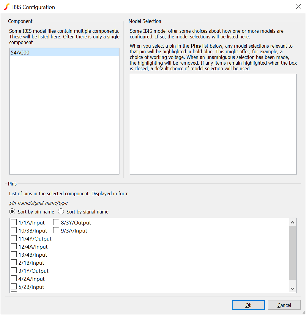
- The Component group at the top left lists the components found in the model file. Often there is only a single component but some IBIS files contain multiple components typically to offer package variations for a given part. Select the component of interest
- The Pins group lists the component's pins. Each entry has three values: pin name, signal name and model type separated by forward slashes. The pin name is typically the package pin number while the signal name describes the purpose of the pin. The model type may be one of Input, Output, I_O, Open_drain, Open_source, I_O_Open_drain, I_O_Open_source, 3-state and Terminator. Select the pins you wish to model. SIMetrix will create a schematic symbol based on your selections
- Some models offer model selections which you will see listed in the Model Selection group at the top right. Typically model selections offer alternative supply voltages or device configurations. When you make your pin selections (see above) they may become highlighted in blue along with one or more of the available model selections. This means that the selected pin or pins have alternative models which you can select by checking one or more of the highlighted model selections. Once an unambiguous model selection has been made, all highlighted elements will be cleared.
- Pres Ok to create and place the symbol on the schematic
With the example shown above, the following picture shows the generated symbol if pins 10 and 11 are selected (signals 3B and 4Y):
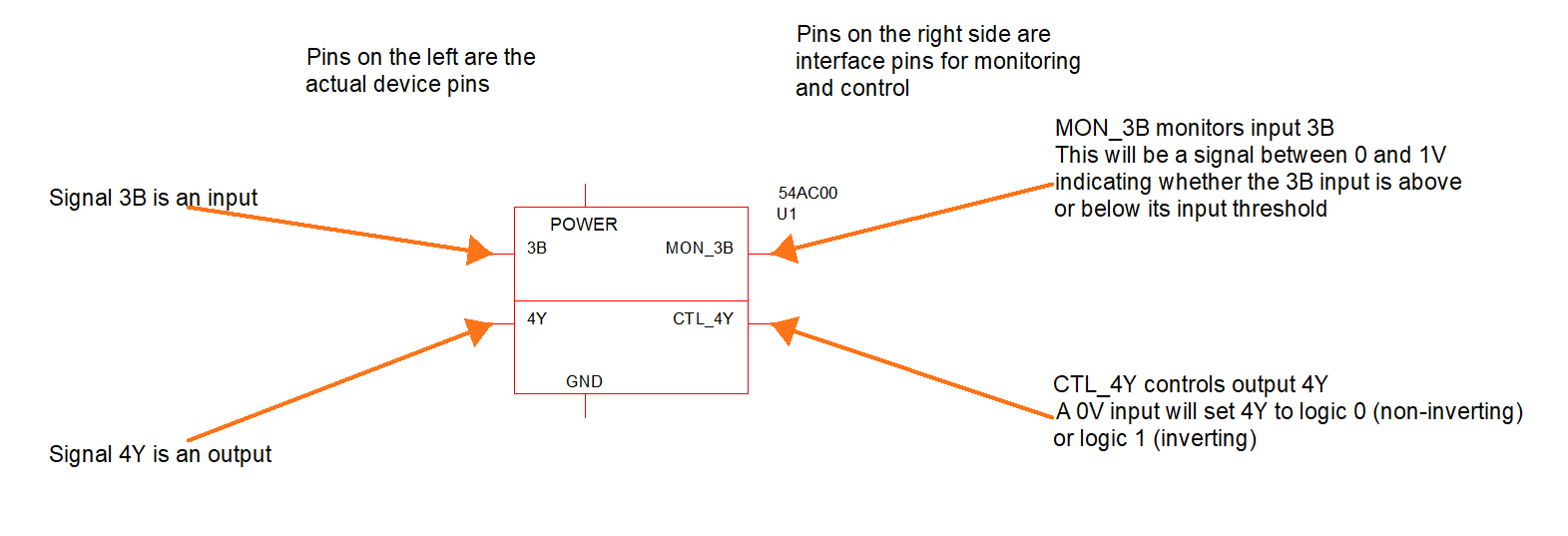
IBIS symbols have two groups of pins. Pins on the left are the actual device pins as listed in the dialog box described above. Pins on the right are interface pins used to interact with the IBIS model. In the above example, 3B and 4Y are the actual pins which are an input and an output respectively. MON_3B is an output which reflects the signal detected at 3B, while CTL_4Y is an input that controls the 4Y output. Both interface pins operate at 0V and 1V signal levels; 0V represents a logic 0 and 1V represents a logic 1.
Some IBIS model types have an enable pin that enables a 3-state output or for an IO pin, the signal direction. These also operate at 0V and 1V.
SIMetrix IBIS models require the connection of a power and ground signal. Each IBIS model is designed to operate at a single supply voltage and the Power signal is expected to be connected to a voltage source set at that voltage.
IBIS Example
A demonstration IBIS file is provided in the standard examples at SIMetrix/IBIS/simetrix_demonstration.ibs. The following describes how to create a simple IBIS schematic based on this model.
- Create a new empty schematic then save it to a suitable directory such as the IBIS example directory itself
- Select menu
- Navigate to the directory SIMetrix/IBIS then select the file simetrix_demonstration.ibs. (The examples folder will usually be available in the file viewer)
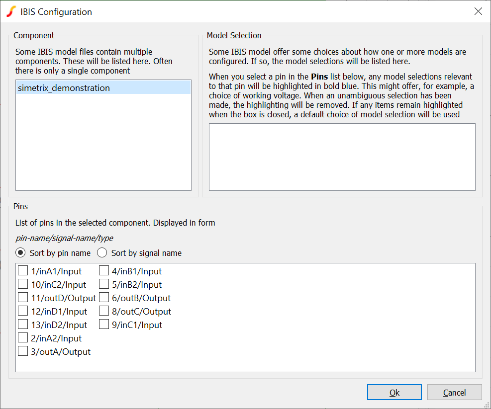
- Click on simetrix_demonstration in the Component box at the top left
-
You should now see this:
-
Check the items labelled 1/inA1/Input and 3/outA/Output as shown below:
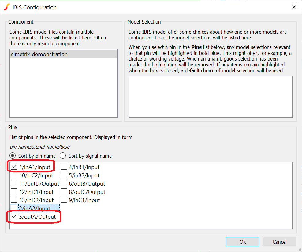
- Click Ok then place the symbol generated
-
Connect up the schematic as shown below:
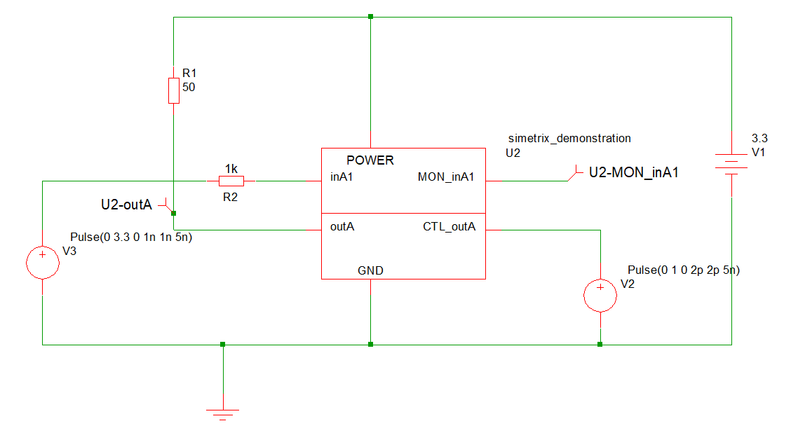
- Setup a 10ns transient analysis and also set a 10ps maximum timestep (Simulator | Choose Analysis... Transient tab -> Advanced Option -> Time step -> Max time step)
- Run simulation. Probe U1-outA is the waveform on an output pin while U1-MON_inA1 is monitoring the input. 0.0V represents a logic zero on the input, 1.0V represents a logic one. 0.5V means that the input state is indeterminate which will occur when the input is between the lower and upper thresholds that determine the input's logic state
Example Notes
- When the IBIS symbol and model are created, an HTML file is also created provided some information about the generated model. In this example the file is called IBIS_simetrix_demonstration_178888575_INFO.html.
- SIMetrix IBIS models require a power supply to be connected.
IBIS Packages
IBIS Models include a model of the physical package that houses the active chip. Some models contain multiple package models for different package types. (E.g TSOP, SO etc)
SIMetrix can create a schematic symbol and electrical model for the specified package. Unlike the IBIS model, the package must be instantiated complete with all device pins.
Instantiating an IBIS Package
- Select menu
- Navigate to a .ibs file
- You will be presented with a list of packages found in the model. Often there is only one. Check the item required
- A symbol will be created and presented for placing. The symbol will have pins on the left marked "IN..." and pins on the right side marked "OUT...". "IN..." pins are pins that connect externaly while "OUT..." pins connect internally to the modelled chip. The REF pin is the AC reference connection to which all capacitors in the package model are connected. It must be connected to something with a DC path to ground but this can be a through a high value resistor
| ◄ Special Parts | Parameters and Expressions ▶ |