The S/R Flip-Flop with Set/Reset models a generic clocked S/R Flip-Flop with either
asynchronous or synchronous set and reset inputs. The Q and QN outputs can
change state only on the specified clock edge unless the asynchronous set or reset is
asserted. The clock edge trigger can be set with the Trigger Condition parameter to
be either rising edge ( 0_TO_1 ) or falling edge ( 1_TO_0 ). If set and reset inputs are
not required, the S/R Flip-Flop can be used.
| Model Name: |
S/R Flip-Flop with
Set/Reset |
| Simulator: |
 |
This device is compatible with the SIMPLIS simulator. |
| Parts Selector Menu
Location: |
|
| Symbol Library: |
None - the symbol is
automatically generated when placed or edited. |
| Model Library: |
SIMPLIS_DIGI1.LB |
| Subcircuit Names: |
- SIMPLIS_DIGI1_SRFF_SR_N : Without Ground Reference
- SIMPLIS_DIGI1_SRFF_SR_Y : With Ground Reference
|
| Symbols: |
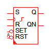 |
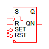
Rising edge triggered,
asychronous set/reset, without ground
reference. |
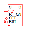 |
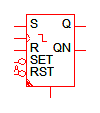
Rising edge triggered,
asychronous set/reset, with ground
reference. |
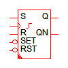 |
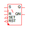
Rising edge triggered,
sychronous set/reset, without ground
reference. |
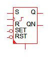 |
Rising edge triggered,
sychronous set/reset, with ground
reference. |
 |
Falling edge triggered,
asychronous set/reset, without ground
reference. |
 |
Falling edge triggered,
asychronous set/reset, with ground
reference. |
 |
Falling edge triggered,
sychronous set/reset, without ground
reference. |
 |
Falling edge triggered,
sychronous set/reset, with ground
reference. |
|
| Multiple
Selections: |
Only one device at a time
can be edited. |
Editing the S/R
Flip-Flop with Set/Reset
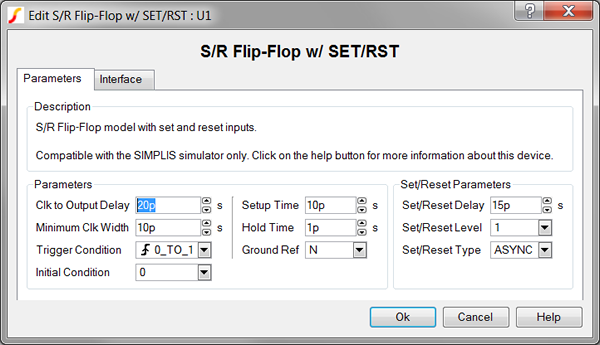
To configure the S/R Flip-Flop with Set/Reset,
follow these steps:
- Double click the symbol on the schematic to open the editing dialog to the Parameters tab.
- Make the appropriate changes to the fields described in the table below the
image.
| Label |
Parameter
Description |
| Clock to Output
Delay |
Delay from the
triggering clock event until the Flip-Flop outputs change |
| Minimum Clk
Width |
Minimum valid clock
width. Clock widths less than this parameter will not trigger the
Flip-Flop. |
| Trigger
Condition |
Determines the
triggering condition of the Flip-Flop clock pin:
- 0_TO_1 for rising edge triggered
- 1_TO_0 for falling edge triggered
|
| Initial
Condition |
Initial condition of
the Flip-Flop output at time=0 |
| Setup Time |
Minimum time before
the triggering clock event that the input signals must remain
steady so that a valid change in each input state is
recognized. |
| Hold Time |
Minimum time after
the triggering clock event that the input signals must remain
steady so that a valid change in each input state is
recognized. |
| Ground Ref |
Determines whether or
not a device has a ground reference pin. Any digital component that
has an input or output pin connected to an analog circuit node must
have its Ground Ref pin connected to an analog node. This is
usually the ground on the schematic. |
| Set/Reset Delay |
Delay from when the SET
or RST pin goes active until the Q output is actually set or
reset. |
| Set/Reset Level |
Determines the
Set/Reset level of a device:
- 1 means active high
- 0 means active low
|
| Set/Reset Type |
Determines whether or
not output events are synchronized with a clock event:
| Set/Reset
Type |
Description |
| SYNC |
Set/reset events are synchronized to the
clock edge defined by the Trigger Condition
parameter. |
| ASYNC |
Set/reset events are asynchronous to the
clock edge. |
|
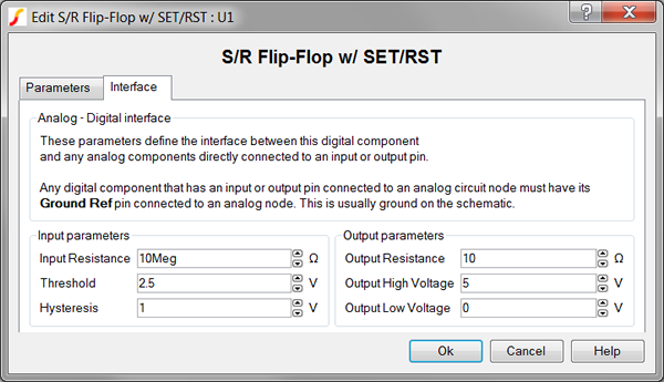
To define the parameters for the interface between this digital component and
each analog component connected directly to an input or output pin, follow these
steps:
- From the Edit S/R Flip-Flop with Set/Reset dialog box, click on the Interface tab.
- Make the appropriate changes to the fields described in the table below the
image.
| Label |
Parameter
Description |
| Input
Resistance |
Input resistance of
each Flip-Flop input pin |
| Hysteresis,
Threshold |
 |
Hysteresis and
Threshold of the inputs. The hysteretic-window width, HYSTWD
is centered around Threshold (TH) voltage. To
determine the actual threshold ( TL , THI ),
substitute Threshold (TH) and Hysteresis
(HYSTWD) in each of the following formulas:
| Input Logic Level |
Actual Threshold |
| 1 |
Threshold + 0.5 *
Hysteresis |
| 0 |
Threshold - 0.5 *
Hysteresis |
|
| Output
Resistance |
Output resistance of
Q and QN pins |
| Output High
Voltage |
Output high voltage for
Q and QN pins |
| Output Low
Voltage |
Output low voltage for
Q and QN pins |
Truth Table
The following truth table assumes a Trigger Condition=0_TO_1 which represents a rising edge clocked Flip-Flop, Set/Reset level=1, and Set/Reset Type=ASYNC, representing asynchronous set/reset.
Asynchronous Set/Reset
|
Inputs |
Outputs |
Action |
|
S |
R |
CLK |
SET |
RST |
Q |
QN |
|
1 |
0 |
|
0 |
0 |
1 |
0 |
Set the Flip-Flop |
|
0 |
1 |
|
0 |
0 |
0 |
1 |
Reset the Flip-Flop |
|
0 or 1 |
0 or
1 |
0 or
1 |
1 |
0 |
1 |
0 |
Asynchronously set the Flip-Flop |
|
0 or 1 |
0 or
1 |
0 or
1 |
0 |
1 |
0 |
1 |
Asynchronously reset the Flip-Flop |
|
0 or 1 |
0 or
1 |
0 or
1 |
1 |
1 |
Last Q |
Last QN |
Illegal concurrent SET and RST |
The following truth table assumes a Trigger Condition=0_TO_1 which represents a rising edge clocked Flip-Flop, Set/Reset level=1, and Set/Reset Type=SYNC, representing synchronous set/reset.
Synchronous Set/Reset
|
Inputs |
Outputs |
Action |
|
S |
R |
CLK |
SET |
RST |
Q |
QN |
|
1 |
0 |
|
0 |
0 |
1 |
0 |
Set the Flip-Flop |
|
0 |
1 |
|
0 |
0 |
0 |
1 |
Reset the Flip-Flop |
|
0 or 1 |
0 or
1 |
|
1 |
0 |
1 |
0 |
Synchronously set the Flip-Flop |
|
0 or 1 |
0 or
1 |
|
0 |
1 |
0 |
1 |
Synchronously reset the Flip-Flop |
|
0 or 1 |
0 or
1 |
|
1 |
1 |
Last Q |
Last QN |
Illegal concurrent SET and RST |
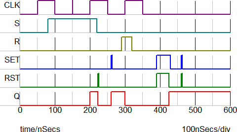
Waveforms
The following waveforms assume Trigger Condition=0_TO_1 which represents a rising edge clocked Flip-Flop, Set/Reset level=1, and Set/Reset Type=ASYNC, representing asynchronous set/reset.
Subcircuit Parameters
The subcircuit parameters, parameter names, data types, ranges, units, and descriptions
are in the following table. The parameter names can be used to directly generate netlist
entries for the device. For example, an
S/R Flip-Flop with Set/Reset
netlist entry without ground reference would be:
X$U1 3 5 2 4 6 7 SIMPLIS_DIGI1_DFF_SR_N vars: IC=0 MIN_CLK=10p TRIG_COND='0_TO_1' CLK_TO_OUT_DELAY=20p SETUP_TIME=10p HOLD_TIME=1p SET_RESET_DELAY=15p SET_RESET_TYPE='ASYNC' SET_RESET_LEVEL=1 GNDREF='N'
| Parameter Name |
Label |
Data Type |
Range |
Units |
Parameter
Description |
| CLK_TO_OUT_DELAY |
Clock to Output
Delay |
Number |
1f to 1024 |
s |
Delay from the triggering
clock event until the Flip-Flop outputs change |
| GNDREF |
Ground Ref |
String |
|
none |
Determines whether or not a
device has a ground reference pin. Any digital component that has an
input or output pin connected to an analog circuit node must have its
Ground Ref pin connected to an analog node. This is usually
the ground on the schematic. |
| HOLD_TIME |
Hold Time |
Number |
1f to 1024 |
s |
Minimum time after
the triggering clock event that the input signals must remain steady so
that a valid change in each input state is recognized. |
HYSTWD,
TH |
Hysteresis,
Threshold |
Number |
min: 1f |
V |
|
Hysteresis and Threshold of
the inputs. The hysteretic-window width, HYSTWD is centered
around Threshold (TH) voltage. To determine the actual
threshold ( TL , THI ), substitute Threshold
(TH) and Hysteresis (HYSTWD) in each of the
following formulas:
| Input Logic Level |
Actual Threshold |
| 1 |
Threshold + 0.5 *
Hysteresis |
| 0 |
Threshold - 0.5 *
Hysteresis |
|
| IC |
Initial Condition |
Number |
|
none |
Initial condition of the
Flip-Flop output at time=0 |
| MIN_CLK |
Minimum Clk Width |
Number |
1f to 1024 |
s |
Minimum valid clock width.
Clock widths less than this parameter will not trigger the
Flip-Flop. |
| RIN |
Input Resistance |
Number |
min: 100 |
Ω |
Input resistance of each
Flip-Flop input pin |
| ROUT |
Output Resistance |
Number |
min: 1m |
Ω |
Output resistance of
Q and QN pins |
| SETUP_TIME |
Setup Time |
Number |
1f to 1024 |
s |
Minimum time before
the triggering clock event that the input signals must remain
steady so that a valid change in each input state is recognized. |
| SET_RESET_DELAY |
Set/Reset Delay |
Number |
1f to 1024 |
s |
Delay from when the SET or
RST pin goes active until the Q output is actually set or
reset. |
| SET_RESET_LEVEL |
Set/Reset Level |
Number |
|
none |
Determines the Set/Reset
level of a device:
- 1 means active high
- 0 means active low
|
| SET_RESET_TYPE |
Set/Reset Type |
String |
|
none |
Determines whether or not
output events are synchronized with a clock event:
| Set/Reset Type |
Description |
| SYNC |
Set/reset events are synchronized to the
clock edge defined by the Trigger Condition
parameter. |
| ASYNC |
Set/reset events are asynchronous to the
clock edge. |
|
| TRIG_COND |
Trigger Condition |
String |
|
none |
Determines the triggering
condition of the Flip-Flop clock pin:
- 0_TO_1 for rising edge triggered
- 1_TO_0 for falling edge triggered
|
| VOH |
Output High Voltage |
Number |
any |
V |
Output high voltage for
Q and QN pins |
| VOL |
Output Low Voltage |
Number |
any |
V |
Output low voltage for
Q and QN pins |
